New workflows support DRC fixing, thermal analysis, advanced packaging and process certification across semiconductor design applications.
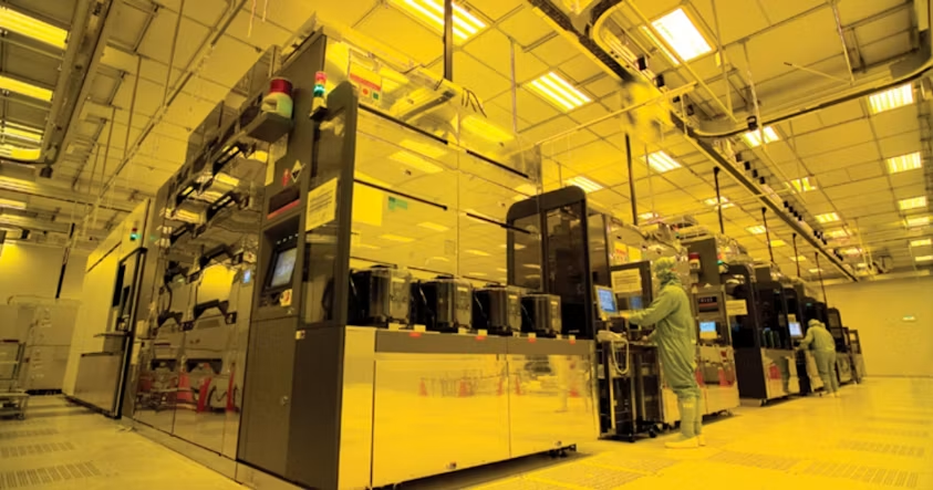
Siemens announced continued collaboration with TSMC on AI-enabled automation and semiconductor design. As part of their work within the TSMC Open Innovation Platform (OIP) ecosystem, the companies are expanding design enablement across semiconductor workflows to support productivity, shorter design cycles and the management of increasing design complexity.
As part of the collaboration, Siemens and TSMC have enabled an AI-powered agent for automated design rule check (DRC) fixing across digital and custom integrated circuit (IC) design flows. The agent uses Calibre software and integrates with Aprisa software and Solido software. It is designed to reduce manual work, support workflow efficiency and help engineering teams progress toward tapeout.
Advancing AI-enabled semiconductor design
Siemens and TSMC are working on AI-enabled semiconductor design using the Fuse EDA AI System and Fuse EDA AI Agent. These technologies support autonomous, long-running and self-verifying electronic design automation (EDA) workflows.
The workflows can handle multi-step design tasks, coordinate actions across EDA tools and validate engineering results during execution. Fuse EDA AI Agent also uses NVIDIA AI technologies to improve token efficiency and support reasoning and execution across extended engineering workloads.
One of the supported applications is an AI-enabled DRC-fix workflow that combines Calibre software, Aprisa AI and Solido Fuse technologies. The workflow is designed to identify, analyze and resolve design rule violations across digital and custom IC design flows.
The workflow builds on Calibre Check Assist, which provides contextual guidance and design rule information during DRC debugging. This can help designers analyze violations and determine corrective actions. The collaboration also includes agentic custom IC design capabilities based on Solido Fuse.
The collaboration includes agentic place-and-route and digital implementation workflows enabled by Aprisa software. These capabilities are intended to automate repetitive tasks, provide domain-specific AI guidance and support design convergence from design creation through tapeout.
Supporting TSMC 3DFabric technologies
Siemens and TSMC are continuing work on 3D IC design enablement for TSMC 3DFabric technologies. Siemens has enabled multi-machine support in Calibre 3DStack Advanced software for inter-chiplet antenna verification, including support for TSMC-SoIC, a wafer-level 3D IC stacking platform.
Certification work is also underway for chip-on-wafer-on-substrate with local silicon interconnect (CoWoS-L). These updates are intended to support the processing and runtime requirements of larger and more complex 3D IC designs. Siemens and TSMC have also evaluated performance improvements in the Interface Check Flow for TSMC-SoW.
Siemens EDA products, including Solido Simulation Suite software, Calibre xACT software and Calibre 3DThermal software, are being used in joint work with TSMC on 3D IC and multiphysics design projects. The work includes silicon photonics applications and other advanced packaging technologies.
Calibre 3DThermal software is certified for static and transient thermal analysis of TSMC 3DFabric technologies. It has also achieved certification for static and transient thermal analysis on TSMC A16 and completed enablement for the system-on-wafer thermal reference flow. Work is underway on the reference flow for TSMC-COUPE, or Compact Universal Photonic Engine.
The companies are continuing work on complete 3Dblox support, including chip-package co-design workflows with mutual customers. Siemens and TSMC are also collaborating on Aprisa software capabilities for pre-simulation-driven die-to-die (D2D) autorouting. These capabilities are intended to help designers develop routing configurations that meet signal integrity requirements.
Siemens EDA technologies have also been enabled for the design, implementation and verification of TSMC-COUPE features. Joint silicon photonics development includes flows based on Innovator3D IC Integrator, Calibre 3DStack, Solido Simulation Suite, L-Edit software and Calibre Interactive.
Solido Simulation Suite software supports PAM4 measurements for optical transceiver interfaces associated with TSMC-COUPE technology. Joint validation of the Calibre 3DThermal solution for TSMC-COUPE is ongoing.
Enabling advanced process technologies
Siemens and TSMC are continuing work on advanced-node certification and design enablement. Calibre nmDRC, Calibre nmLVS, Calibre xACT and Calibre PERC have been certified for the TSMC A14 process node.
Solido Simulation Suite software is certified for SPICE accuracy on TSMC N3C, A16 and A14 process technologies. The certification supports analog, RF and memory verification.
The collaboration also covers TSMC’s custom design reference flow. Siemens technologies support reliability-aware simulation capabilities for IC aging, real-time self-heating and safe operating area checks. Solido Design Environment supports variation-aware verification and automated cell optimization.
mPower software is certified for transistor-level IR/EM analysis on TSMC N2P for digital and analog designs and on TSMC N3C for analog designs. Siemens and TSMC are continuing work on custom design reference flows for electromigration and IR-drop analysis on N2 and N3 technologies.
Certification activities for Aprisa software and mPower analog software on A14 technology are also underway.
Expanding advanced-node design training
Siemens Xcelerator Academy provides self-paced, on-demand training resources for the Siemens EDA portfolio. The program is now available to TSMC Design Center Alliance partners as well as mutual customers.
Siemens recently released an end-to-end digital implementation flow lab tutorial based on TSMC 5nm process technology through the program. The tutorial provides additional training on advanced semiconductor design methods.
For more information, visit siemens.com.