New A14 flows, agentic AI tools, multi-die design capabilities and silicon-proven IP support advanced semiconductor development.
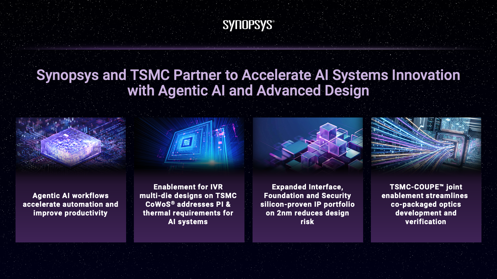
Synopsys announced new collaborations with TSMC focused on the development of AI, high-performance computing (HPC), and advanced semiconductor systems. The companies are combining AI-enabled electronic design automation (EDA) flows, multiphysics-aware signoff methods, multi-die design flows, and silicon-proven Interface and Foundation IP to help customers manage design complexity and adopt TSMC’s latest process and advanced packaging technologies.
Supporting advanced-node adoption and design convergence
Synopsys and TSMC are working to support customer transitions to newer process technologies. Recent developments include A14 certification for digital and analog design flows, along with support for agentic AI capabilities. These certified flows cover implementation through signoff and are intended to support design convergence on TSMC’s A14 technology.
For analog design, Synopsys and TSMC are enabling device routing on A14. This supports analog place-and-route automation and can help improve layout productivity during the adoption of advanced process technologies.
Using agentic AI to improve engineering productivity
Synopsys and TSMC are applying agentic AI to analog, digital, and multi-die design workflows. Synopsys Custom Compiler supports analog migration, while Fusion Compiler uses large language model (LLM)-assisted analysis to support design productivity.
For multi-die designs, the companies have introduced an agentic AI flow for chiplet floorplan co-optimization using the Synopsys 3DIC Compiler platform. The flow automates parts of the floorplanning process and supports design convergence for systems based on TSMC 3DFabric technologies.
Supporting multi-die design and power delivery
The power requirements of newer AI systems are increasing the importance of integrated voltage regulators (IVRs) in multi-die designs. IVRs can support power efficiency and power integrity.
The Synopsys 3DIC Compiler platform enables designers to co-design and simulate IVRs for TSMC CoWoS technology in a unified advanced-packaging environment.
Supporting co-packaged optics design
Optical interconnects are being used to support high-speed connectivity between system components. Synopsys is working with TSMC to support co-packaged optics (CPO) design on TSMC COUPE technology through an integrated photonic and electronic co-design flow.
The flow covers 3DIC implementation, multiphysics analysis and optimization. It is intended to help customers develop and verify optical interconnect architectures for multi-die systems.
Providing silicon-proven IP for AI and other advanced systems
Synopsys and TSMC are providing Interface, Foundation, and Silicon Lifecycle Management (SLM) IP for AI, HPC, data center, edge, and physical AI systems. The IP is optimized for TSMC’s advanced process technologies and builds on first-silicon results for TSMC’s N5, N3P, and N2P technologies.
Synopsys is continuing to expand its IP portfolio to help customers manage design risk, shorten development schedules and address power, performance, and scalability requirements.
For TSMC’s N2P process, Synopsys reported IP enablement and tape-out milestones for AI and HPC applications. These include PCIe 7.0, HBM4, LPDDR6/5X/5, 224G Ethernet PHY, UCIe, OTP, and advanced SLM process, voltage and temperature (PVT) monitoring IP. The solutions support connectivity, memory and system-monitoring requirements for AI workloads.
For multi-die systems, Synopsys demonstrated UCIe-A 32G/40G silicon on a TSMC N3P test chip integrated with a CoWoS-S interposer. The demonstration validated die-to-die connectivity for AI system designs. Synopsys also completed 64G UCIe IP tape-outs on 2nm and 3nm process nodes. The IP includes embedded design-for-test (DFT) capabilities for in-system visibility.
Synopsys has also expanded its silicon-proven Foundation, MIPI, and memory IP for TSMC’s N3P and N2P processes. The company is developing additional IP for TSMC’s compact “C” process technologies from 6nm through 3nm. These solutions support system integration and power-efficiency requirements across AI, data center, networking, mobile, automotive and edge AI applications.
For more information, visit synopsys.com.