The OSFP-sized design targets up to 12.8 Tb/s of aggregate capacity with 16 full-duplex lanes for AI factory networks.
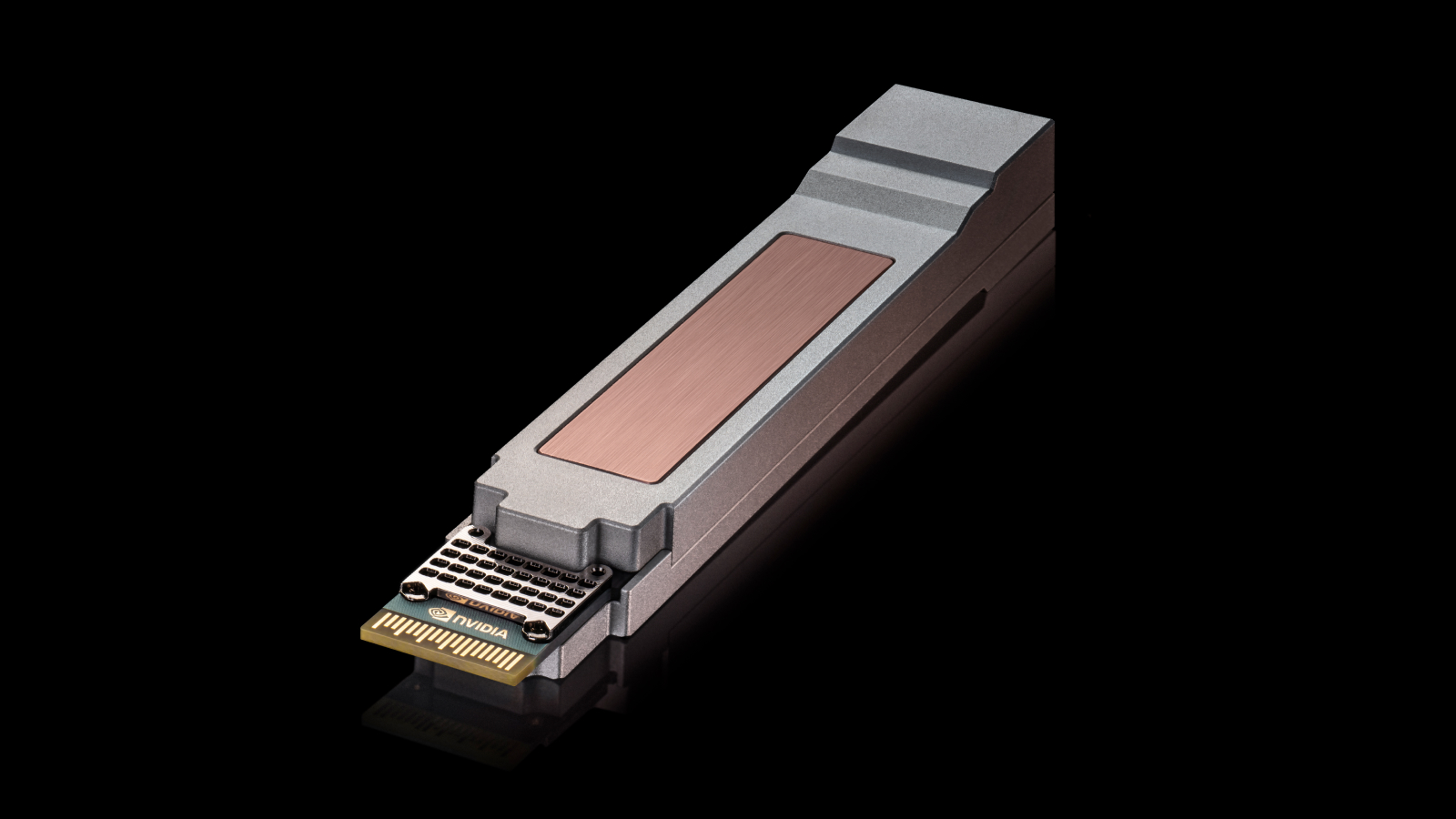
NVIDIA and Cisco announced plans for Ultra-Dense Small Form Factor Pluggable (USFP), a high-density optical module designed to support 400 Gb/s per lane in AI factory networks that use pluggable transceivers.
As AI models and inference workloads expand, AI factories need to connect more computing systems while managing network complexity, power consumption and costs. Increasing the amount of data transmitted per watt and per switch can help operators use existing infrastructure more efficiently.
Scaling AI factories requires higher bandwidth per connection and more connections per switch. Once a switch reaches its capacity, expanding the network may require additional switch layers and optical links, which can increase latency, power consumption and costs.
USFP is designed to support the transition from 200 Gb/s-per-lane to 400 Gb/s-per-lane Ethernet AI fabrics. It uses a pluggable transceiver model that has been deployed across multiple generations of data center networks, allowing customers to adopt higher-bandwidth optical technology without replacing their entire data center infrastructure.
The first planned USFP transceivers will include 16 full-duplex lanes in an octal small form factor (OSFP)-sized footprint for use with switches and SuperNICs. The design can support future versions with 32 or more lanes. By increasing both the lane count and bandwidth per lane, USFP is designed to connect more 1.6 Tb/s endpoints without adding network tiers. The planned configuration will provide up to 12.8 Tb/s of aggregate capacity.
In an OSFP-sized module, USFP is specified to provide four times the bandwidth and front-panel bandwidth density and approximately 1.3 times the power efficiency of 200 Gb/s-per-lane pluggable modules. This can allow AI infrastructure designers to increase compute capacity within the same network footprint while reducing the proportion of the AI factory power budget used by networking.
Increasing switch capacity
USFP is designed for electrical signals of 400 Gb/s per lane and uses a two-dimensional array connector with a two-step insertion process. High-speed contacts engage after the module is inserted, which is intended to reduce contact wear and support signal integrity while making insertion force more consistent.
The connector supports future versions with 32 full-duplex lanes or more. Because it is designed for 400 Gb/s operation, it can also support improved performance at 200 Gb/s per lane.
USFP supports power dissipation of up to 100 watts without a separate embedded cooling circuit inside the transceiver. This can reduce switch design requirements while supporting the use of pluggable transceivers. The design is intended to support higher-bandwidth networks while maintaining the deployment, serviceability and manufacturing processes used for existing pluggable transceivers.
USFP configurations support optical designs that can reduce latency and power consumption by simplifying signal processing. Support for different optical technologies and connection distances gives system designers options for adapting the modules to specific AI factory network requirements.
Developing an ecosystem for AI factory networks
NVIDIA and Cisco are working with TE Connectivity and Amphenol to develop USFP cages, connectors and modules. Additional companies may participate in the effort. The shared form factor is intended to give suppliers a common basis for developing pluggable infrastructure for 400 Gb/s-per-lane networks.
The collaboration builds on NVIDIA and Cisco’s work to support interoperability between NVIDIA Spectrum-X Ethernet networking and Cisco Silicon One-based Ethernet networks. The companies intend to support deployments by enterprises, neoclouds and sovereign clouds.
NVIDIA and Cisco plan to develop an open industry specification for USFP through a community-led, multisource project.
For more information, visit nvidia.com.